Parylene conformal coating is suitable for metals, elastomers, electronics, and plastics and is used extensively in the automotive, aerospace, electronics, and medical industries. Parylene coating is an ultra-thin film polymer coating that provides a uniform pin-hole-free barrier coating to all shapes, edges, crevices, and recesses with the same thickness without suffering any of the edge effects of conventional coatings.
Parylene Coating can be applied to various materials, such as substrates, plastics, metals, elastomers, electronic components, and assemblies.
Parylene Conformal Coating Process
Parylene coating is performed in white and clean room facilities with custom-designed equipment and is derived from proprietary dimers. Parylene is applied under vacuum by vapor deposition at room temperature.
Stage 1 – SUBLIMATION: The dimer is heated in a partial vacuum to 150° C, converting from a solid to a gaseous state. The amount and purity of the dimer used dictate coating thickness and uniformity. Our proprietary dimers are 99.6% pure.
Stage 2 – PYROLYSIS: A gaseous dimer is heated in a furnace. As the temperature rises, the molecular structure changes and begins to crack or break down. At over 650° C, the dimer is split into monomers.
Stage 3 – POLYMERIZATION – In the deposition chamber, where the coating of the customer-provided product occurs, the coated parts are maintained at room temperature. Still, the monomer is drawn into the chamber in its gaseous phase and undergoes polymerization. The nanoparticles combine chemically to provide a chainlike or network molecule. At a rate of 1-2 microns per hour, a single clear coating builds up one molecule at a time, encapsulating all exposed surfaces. Controlled coating thicknesses ranging from less than 10 nanometers to 70 microns are achieved in a single operation.
Two Chamber Coating Designs
Monomer flow is directed tangentially to the chamber load using a proprietary fixture design to enhance diffusion and coating uniformity while minimizing raw material consumption.
Variable Aperture Plates are below the fixtured parts. These plates are pre-adjusted based on the volume and geometry of each chamber load to achieve a uniform and effective deposition.
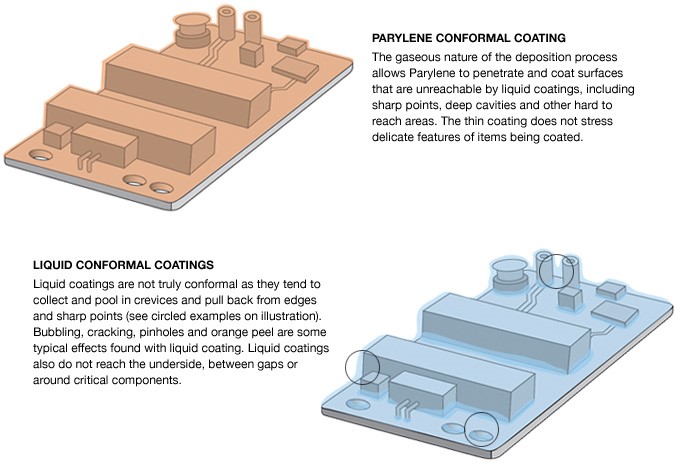
Parylene Conformal Coating versus Liquid Conformal Coating
CWST announced that its location in Aliso Viejo, CA, has added liquid coating capability to its conformal coatings family of services. Learn more about acrylic & urethane conformal coating.
Biocompatibility and Bio-Stability (can be sterilized)
Optical Clarity
Zero Outgassing of Volatile Chemicals
Added Values
The Parylene coating process does not include a liquid phase. Thus, the coating will not pool in low areas, bridge across substrate features, or exhibit liquid properties such as meniscus or capillary action.
Parylene film is a pure, polycrystalline, and amorphous linear polymer distinguished by superior dielectric, gas barrier, and mechanical properties. These properties allow it to meet coating requirements in very thin layers.
Low static and dynamic coefficients of friction, giving it dry film lubricity that can be valuable for some applications.
The room-temperature deposition process makes Parylene coating suitable for many substrates, including ferrites, rubbers, silicone elastomers, paper, resins, plastics, silicon, metals, and even granular material
Since Parylene coating is highly effective in very thin coating applications, delicate substrates such as electronic sensors or diaphragms can be protected without significant mechanical or loading effects.
Parylene Coating – Dimer Supplier
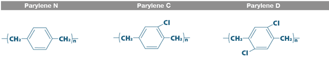
Parylene raw materials are called dimers. CWST offers IPC-CC-830 and USP Class VI-approved Parylene dimers. These are the key raw materials used in the Parylene coating process. The most common types of commercial parylene raw materials or dimers are Dimer C and Dimer N. Learn more about parylene dimers.
Parylene Conformal Coating Methods
There are two types of Parylene coating methods: fixed coating and tumble coating. The method chosen depends on whether the part needs selective or evenly coated parylene coating coverage. Learn more about parylene coating methods.
The unique Parylene polymer series was isolated by a research chemist in the late 1940s at the University of Manchester in England. Union Carbide Corporation scientist William Gorham later developed a deposition process to apply the film, and Union Carbide commercialized the material and process. CWST Para Tech Coating purchased licensing for this coating process in 1968 and subsequently developed and patented several important enhancements that optimize the performance, consistency, and reliability of Parylene vacuum deposition coating.
Conformal Coating Machines
Curtiss-Wright Surface Technologies can provide spare parts, critical components, and materials for the operation of Parylene coating machines. Our expert team can provide technical support to troubleshoot and repair coating equipment.
Parylene Coating FAQs
Is parylene coating safe for the environment?
Parylene is green chemistry, it produces no cut forces, no thermal stresses, or leachable ingredients.
Is the parylene coating conformal?
Stable for any substrate stable in a partial vacuum environment, regardless of the topography of the substrate and purity of the dimer, the deposition process ensures a truly conformal coating.
What does parylene coating do?
Parylene ruggedizes electronic components and assemblies. It has excellent diametric strength, suppresses tin whisker growth, and significantly improves lead-free solder joint life. Chemically inert, ROHAS, and reach compliant, it encapsulates the product with a protective barrier, repelling corrosive chemicals, gases, moisture, and liquid.
Can electronics be coated with parylene?
Parylene is the coating of choice for high-reliability electronics.
Can parylene be used for coating medical devices?
For medical device manufacturing aids and delivery systems, parylene is used extensively to provide particulate-free, bio-compatible dry-film lubricity.
What is the benefit of parylene coating?
Parylene removes the tackiness of elastomeric parts without adding weight or materially affecting the substrate’s elasticity. Sealing porosity, elastomers coated with parylene benefit from its low coefficient of friction and its biocompatible and environmentally protected layer.